Create your own PCB
12/03/2020 -
You can create your own PCB, it is easier than it looks.
Software
Because I share pictures of board layouts I am working on, a frequent question I get on instagram is "what is that program you are using?"
It's EaglePCB. There are other programs and there is really not much between them, choose your weapon and stick with it, although it is fairly easy to move from one to the other - once you master the basics. Kicad is also popular, and I actually started out messing about with EasyEDA which is also excellent, and is a web application, but I had issues logging in to the desktop version.
All of these are FREE as in beer! download them, sign up, start making mistakes - you gotta make mistakes to learn! Start with something simple - a boost circuit - and start figuring out how it all works. Once you know the basics you'll want to do more and you'll learn more.
Datasheets
One piece of advice I'd give you is to learn how to read datasheets. It is vital to know the specs of the components you will be using. Not only the electrical specifications, but also the physical dimensions, pin layouts etc. When you are creating your circuit schematic you will need to pick suitable components. Resistors are simple enough, electrolytic capacitors can be bulky so you'll need to know which case is best, ICs have their own requirements, and surface mount components have a bewildering choice of sizes.
Create your own library
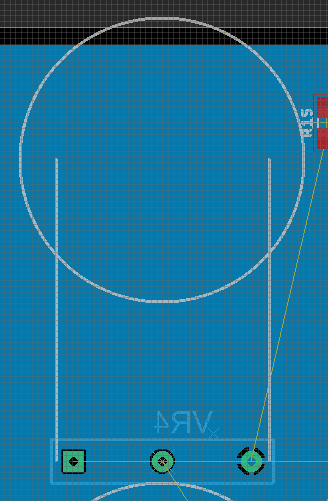
Often the component you want to add will not have a footprint or symbol that you require, or it might have the right schematic symbol but the foot print is not quite right. I had that issue with potentiometers - I wanted to represent the physical size of a specific type of potentiometer from musikding.de that I wanted to use. In this case the physical dimensions are described rather than shown in a diagram, but it was possible to generate what I wanted - you can too, just a little patience.
Grid Measurements
When you are laying out the board it will be on a grid that is usually a 50 mil spacing - that is mil which is a thousandth of an inch and NOT a millimeter.
This is important when you are creating your own components as I mentioned above, because most component's physical measurements are provided in millimeters (metric) and the grid to lay them out is mils / thousandths of an inch (imperial). Pay attention and learn how to swap the grid measurement when you need to, and you will need to do it a lot.
Fabbing
I'm not going to run through how to generate the files needed to send to a fabrication plant to allow them build your creations, I'm just going to mention a few places I know of.
JLCPCB
The jlcpcb.com factory is based in China and does really, really excellent work. They are fast and very cheap, and will even assemble your components onto your board for you, although I only recommend you do that with surface-mount designs.
OSH Park
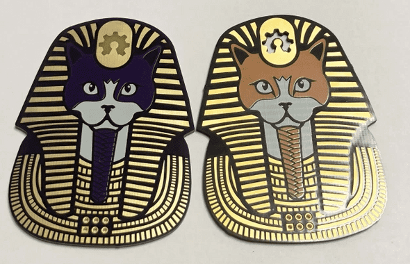
Osh park is based in the USA and while it does not do assembly, that I know of, it has some truly beautiful board selections - checkout "after dark" - yes, this is a circuit board!
Choose the JFET life
Jump in and start making mistakes as I said - with software you can easily correct it and try again, just make sure you use your design software's built-in error checking tools which will warn you if your design has overlapping wires etc.


